Apple will be first to receive 3nm chips from TSMC, but not for the device you’re thinking of

The world’s leading foundry is Taiwan Semiconductor Manufacturing Company, Limited (TSMC). Both it and Samsung are shipping chips this year made using their 3nm process node. The smaller the process node, the higher the transistor count in chips. With the iPhone 14 series expected to be released around the second week of September, Apple will use the 4nm A16 Bionic to power the expensive Pro models while the currently used 5nm A15 Bionic chip will be used on the non-Pro models.
Samsung has already started shipping chips made with its 3nm process node
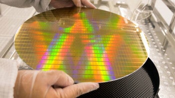
The reason why this is important is that the larger the transistor count, the more powerful and energy-efficient a chip is. Samsung Foundry has already started shipping out 3nm chips this year, but only for cryptocurrency miners. TSMC will also ship 3nm chips this year and with Apple the firm’s largest customer, you would expect the tech giant to be the first to receive N3 chips from TSMC when they start shipping later this year. N3 is the designation for TSMC’s first generation of 3nm chips.
TSMC will reportedly ship its first 3nm chips to Apple later this year
When can we expect to see TSMC producing 2nm chips?
So what happens after 3nm? This past April, TSMC CEO C.C. Wei said that the target is for TSMC to start shipping 2nm chips by 2026 making 3nm “a long node.” Most nodes last for two years. While TSMC is still using FinFET transistors at 3nm, it will switch to Gate-All-Around for 2nm, a switch that rival Samsung already made with its 3nm node. Both foundries will continue to use Extreme Ultraviolet Lithography (EUV) on their 3nm nodes to etch the thinner than hair circuitry patterns on the wafers that become chips.
But let’s not get too ahead of ourselves. TSMC says that its 3nm FinFET chips will reduce energy consumption by 25-30% at the same speed, and increase speed by 10-15% at the same amount of power compared to its previous 5nm FinFET chips. Samsung has said that its 3nm process node will reduce energy consumption by 45%, and improve performance by 23%.